A91x9M0 SLPTimer喚醒後 Write/Read AT24C02 EEPRom
回顧之前提到的當A9139M0進入PM2喚醒後,因為I/O處於高阻抗狀態,需要手動設定I/O Control寄存器為Normal (Ref:PM2喚醒後I/O失效問題解決)
本篇製作一款使用Atmel的AT24C02 EEPRom,存储容量2K bit,内容分为323页,每页8Byte,共256Byte(詳細規格書可自行上網搜尋),底下介紹使用A9139M0的SleepTimer喚醒後,對此顆做I2C Write & Read EEPRom內容的Demo 。
代碼:< RC_A9139M0_x1_433MHz Band Ref. Code_NonRF_V0.5_Test SleepTimer I2CWrite&Read AT24C02 EEPROM_0605.zip>
1.PM2 喚醒後先Unlook Power Reg並將I2C P0.4 & P0.5設為Normal Mode
    while(1)
        {
            //Unlook Power Reg
            POWER->PWR_TA = 0xAAAAAAAA;
            POWER->PWR_TA = 0x55555555;
            POWER->IO_CTRL0 = 0x00000030; //P0.04 & P0.05 set normal
2. 初始化I2C,並設定要寫入的Address,這裡使用0x50
            I2CM_Initial(I2CM, 1);                  // SCK speed = Fsys/2/10/(1+0)
            GPIO0->ALTFUNCSET = (1<<4) | (1<<5);  // set I2C IO
            I2CM_Setup(I2CM, 0x50, 1);                      // setup slave address = 0x50, 1=Write mode
3.依序執行Start==>Address==>等待ack ok==>write data1~data4
            if(0 == I2CM_Send(I2CM, 0x0A, START | RUN))     // send START and data (0x0A)
	    {
                I2CM_Send(I2CM, 0x01, RUN);                 // send data (0x01)
                I2CM_Send(I2CM, 0x02, RUN);                 // send data (0x02)
                I2CM_Send(I2CM, 0x03, RUN);                 // send data (0x03)
                I2CM_Send(I2CM, 0x04, RUN | STOP);          // send data (0x04) and STOP
       	    }
4. Read Address 0x50看看是否寫入成功0x01,0x02,0x03,0x04 資料,讀之前一樣需要先對0x50Address做寫入Start命令,才能切換到Read Mode
            I2CM_Setup(I2CM, 0x50, 1);                      // setup slave address = 0x51, Write mode
            if(0 == I2CM_Send(I2CM, 0x0A, START | RUN))     // send START and data (0x0A)
	    {
                I2CM_Setup(I2CM, 0x50, 0);                  // setup slave address = 0x51, 0=Read mode
            if(0 == I2CM_Read(I2CM, &Buffer[0], START | RUN | ACK)) // send START and read data with ACK
                {
                    I2CM_Read(I2CM, &Buffer[1], RUN | ACK); // read data with ACK
                    I2CM_Read(I2CM, &Buffer[2], RUN | ACK); // read data with ACK
                    I2CM_Read(I2CM, &Buffer[3], RUN | STOP);// read data with "NAK" and send "STOP"
                }
	    }
5.再次進入PM2,等待下次喚醒
			PM2();
	}
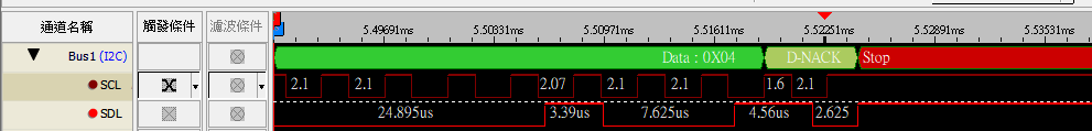
實測邏輯分析圖:
Write部分:


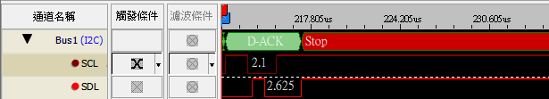
Read 部分: